Table of Contents
FIC 386SC
A nice, clean working 386DX motherboard supporting cache and a range of clock speeds… with a big plus of not using a barrel battery!
Initial Thoughts
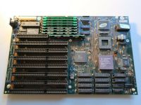
This was a spur-of-the-moment purchase from Ebay in April 2021. I was just browsing through my normal searches for old PC kit and found this board, at first I was interested in looking it up on the Ultimate Hardware 2019 site to see what the chipset was capable of. I saw it was a pretty capable chipset and then did a few searches on Vogons.org to see if anyone else had any experience of it… I couldn't find any, but did find a few other boards (mainly DTK motherboards) using the same chipset, and reports of very solid performance.
At the relatively modest price for a clean, undamaged 386DX board, I thought it worth a go….
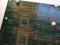
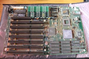
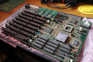
Original Auction Images
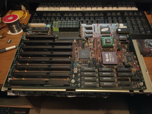
Some observations:
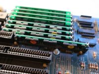
- Has 8MB of 1MB SIMM's fitted
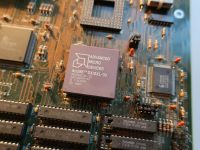
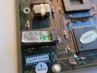
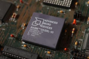
- Has a 33MHz AMD 386DX fitted - but it's unclear if this is socketed or soldered; may have to be removed
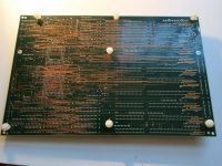
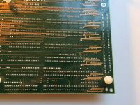
- Clean, no visible damage
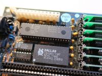
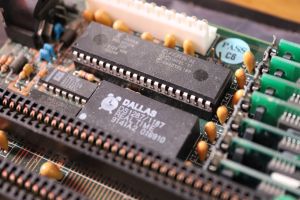
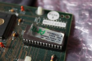
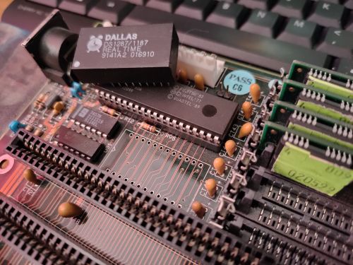
- Uses a Dallas RTC module, rather than the more common barrel battery - no corrosion, but the RTC is likely to be flat
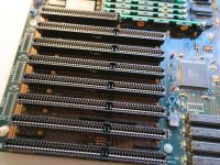
- 7 full 16bit slots, plus 1 8bit slot; that's on the generous side for a 386
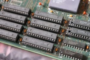
- 8 cache sockets, can't quite make out the capacity, but should be either 128 or 256KB
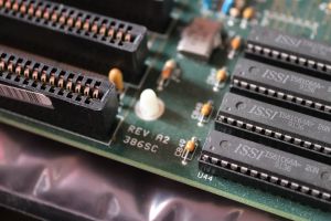
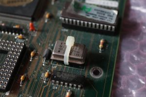
[Update - 29/04/2021] - On arrival and closer inspection of the cache SRAM chips, they total a capacity of 64KB, not 256KB. They're also 20ns, so could do with being exchanged for 15ns parts in order to run them at 0ws with the faster 40MHz processor(s) I intend to fit. But a bonus is that the processor is socketed, as is the main clock crystal - so no soldering needed at all with this board.
Arrival Pictures
Motherboard Data & Variants
A summary of the motherboard capabilities follows:
| Item | FIC 386SC | |
|---|---|---|
| Form Factor | Baby AT | |
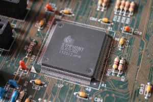
| Chipset | Symphony Labs SL82C360 (Haydn II [Cache]) | |
| Dimensions | 330mm x 218mm | |
| Maximum RAM | 32MB (8x30pin) | |
| Cache | 0,32,64,128,256KB | |
| FPU | 387, Weitek 3167 | |
| CPU Type | 386 DX | |
| CPU Speeds | 25, 33, 40MHz | |
| Expansion | 7x16bit, 1x8bit | |
For the provision of UMB regions to load drivers and TSR applications outside of base 640KB, the The Last Byte memory manager supports the chipset and can provide up to 256KB of UMB regions (configured as 8x 16k + 2x 64k):
Initial Testing
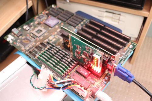
With just a basic VGA card and a POST diagnostic card the system powered straight up:
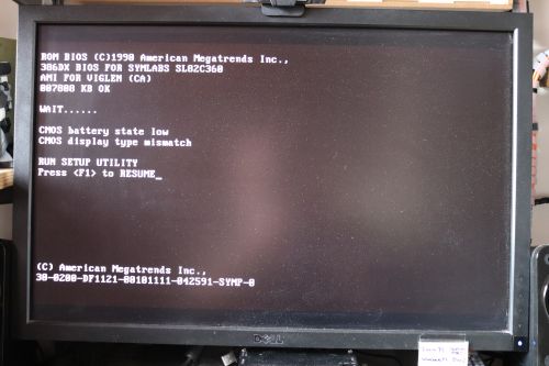
The Dallas RTC is flat, as expected, but other than that it all seems to work.
Note: One odd bit of behaviour is that no diagnostic codes are shown on the POST card at all - you usually see them flash by during the initial power on.
Repairs
Dallas RTC Replacement
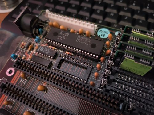
Desolder the failed RTC module:
DIP socket fitted to make future replacement of the RTC easier:
RTC not yet fitted, but board now complete and fitted to the chassis mounting panel, ready to be installed into the case:
Modifications
Clock Speed
Installation of 80MHz oscillator.
Easy job - just cut the zip-tie holding the original 66MHz oscillator off, and push in the new 80MHz part. No modifications necessary.
Cache Upgrade
The cache as-fitted to the board was made up of eight 64kbit x 8bit SRAM modules with two 16kbit x 4bit TAG SRAM modules.
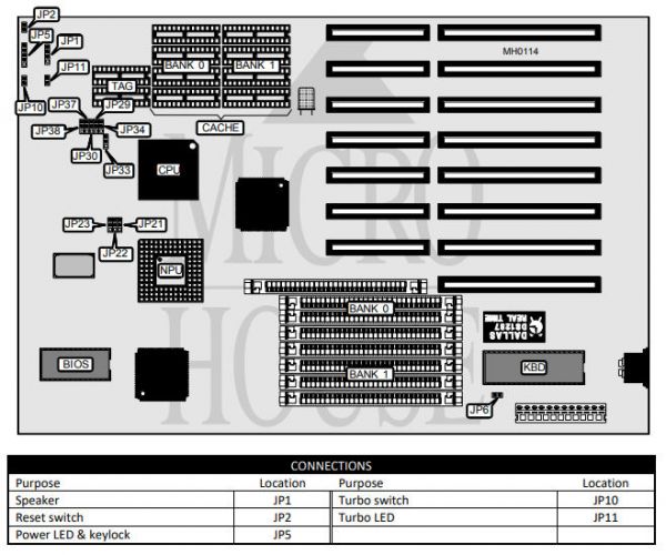
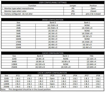
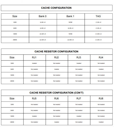
Unfortunately both the configuration of the on-board cache setting jumpers as well as the type and size of the TAG SRAM modules for a 256KB cache setup is not defined. Neither the TH99 or UH19 websites list the settings for this “revision A” of the FIC 386-SC.
[Update - 11/05/2021] - The correct parts for a working 256KB configuration are:
- Eight modules of 32k by 8bit (256kbit) cache SRAM (e.g. UMC UM61M256K)
- Two modules of 64k by 4bit (256kbit) TAG SRAM (e.g Samsung KM64258BP)
In addition, the correct jumper settings, again for an A2 board, are:
- JP34: 2-3
- JP29: 2-3
- JP30: 2-3
- JP37: 1-2
- JP38: 2-3
Configuration
Link to the motherboard data on the following sites:
- Ultimate Hardware 2019 - as the FIC 386SC (Revision A2)
- Ultimate Hardware 2019 - as the FIC 386SC/386-SC (Revision B)
- Total Hardware 99 - as the FIRST INTERNATIONAL COMPUTER, INC. 80386DX-SC (REV. B)
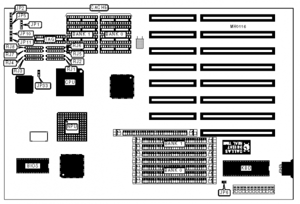
Board Configuration
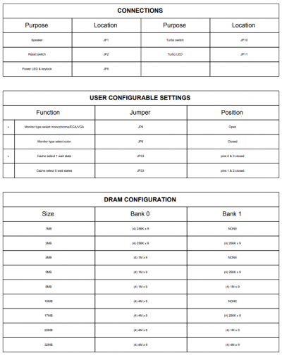
There are some minor differences between the A2 and B revisions, mainly in the configuration of the cache memory.
Revision "A2"
Revision "B"
BIOS Images
Original BIOS files:
MR BIOS files:
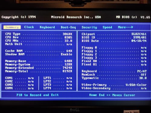
The alternative MR BIOS image appears to run fine on this board and gives a slightly better BIOS user interface:
0 Wait State & Further BIOS Optimisation
Math Co-Processor
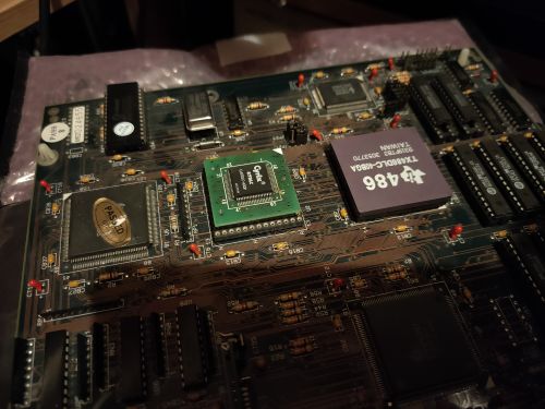
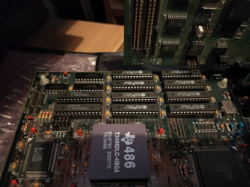
486DLC Processor
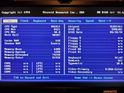
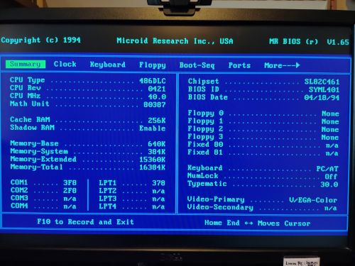
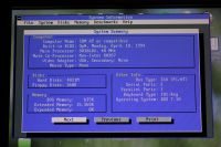
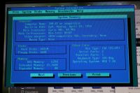
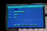
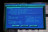
The MR BIOS rom image for this board has native support for the Cyrix/Texas Instruments 486DLC and identifies the process as such in the BIOS info screen:
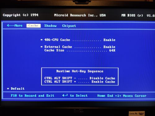
It also features built-in support to enable/disable the DLC on-chip cache from within the BIOS:
256KB Cache
To configure 256KB cache on this Revision A2 board requires the following setup:
- (8x) 32k x8 (256kbit) SRAM cache modules
- (2x) 64k x4 (256kbit) SRAM TAG modules
The TAG modules are somewhat unusual in that it needs a pair and that they are 4bit wide… so they are quite hard to find.
In addition, the jumpers on a Revision A2 board should be set as follows:
- JP34: 2-3
- JP29: 2-3
- JP30: 2-3
- JP37: 1-2
- JP38: 2-3
It appears that JP33 configures the cache wait states. By default with 20ns rated parts, my board was set to 2-3 which I believe to mean: 1ws. With 15ns or faster parts you should be able to use 1-2 which is 0ws. Not all boards or SRAM modules may be able to tolerate this - hopefully the benchmarking should identify any instability.
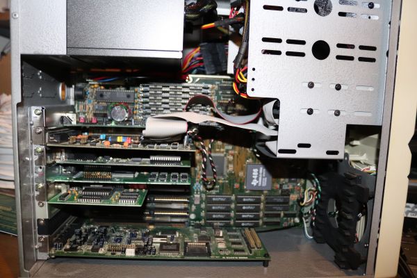
Case Setup
Speed Testing & Tuning
Configuration 0
- AMD Am386DX-40
- Cyrix cx87DLC-40 FPU
- 256KB Cache
- 0 wait states, cache enabled, 10MHz ISA clock, video+system shadow enabled.
- 4x 4MB 60ns SIMMs
- VGA 1 - Trident 9000b 512k VGA
- VGA 2 - Tseng Labs ET4000AX 1MB VGA
- VGA 3 - Cirrus Logic CL-GD5428 1MB VGA
This is the default baseline configuration with the 386DX and sensible BIOS options.
VGA 1
VGA 2
VGA 3
Configuration 1
- AMD Am386DX-40
- Cyrix cx87DLC-40 FPU
- 256KB Cache
- 0 wait states, cache enabled, 13MHz ISA clock, video+system shadow enabled.
- 4x 4MB 60ns SIMMs
- VGA 1 - Trident 9000b 512k VGA
- VGA 2 - Tseng Labs ET4000AX 1MB VGA
- VGA 3 - Cirrus Logic CL-GD5428 1MB VGA
Increased ISA bus speed.
VGA 1
VGA 2
VGA 3
Configuration 2
- Texas Instruments TI486DLC-40 - level 1 cache disabled
- Cyrix cx87DLC-40 FPU
- 128KB Cache
- 0 wait states, cache enabled, 10MHz ISA clock, video+system shadow enabled.
- 4x 4MB 60ns SIMMs
- VGA 1 - Trident 9000b 512k VGA
- VGA 2 - Tseng Labs ET4000AX 1MB VGA
- VGA 3 - Cirrus Logic CL-GD5428 1MB VGA
The first test using the 486DLC processor, albeit at 10MHz bus speed and with internal cache disabled. Any improvements here are likely to be down to the 486 instruction set and microarchitecture.
VGA 1
VGA 2
VGA 3
Configuration 3
- Texas Instruments TI486DLC-40 - level 1 cache enabled
- Cyrix cx87DLC-40 FPU
- 128KB Cache
- 0 wait states, cache enabled, 10MHz ISA clock, video+system shadow enabled.
- 4x 4MB 60ns SIMMs
- VGA 1 - Trident 9000b 512k VGA
- VGA 2 - Tseng Labs ET4000AX 1MB VGA
- VGA 3 - Cirrus Logic CL-GD5428 1MB VGA
Enabling the 486DLC on-chip cache. In theory this should have a substantial performance improvement.
VGA 1
VGA 2
VGA 3
Configuration 4
- Texas Instruments TI486DLC-40 - level 1 cache enabled
- Cyrix cx87DLC-40 FPU
- 128KB Cache
- 0 wait states, cache enabled, 13MHz ISA clock, video+system shadow enabled.
- 4x 4MB 60ns SIMMs
- VGA 1 - Trident 9000b 512k VGA
- VGA 2 - Tseng Labs ET4000AX 1MB VGA
- VGA 3 - Cirrus Logic CL-GD5428 1MB VGA
486 DLC, on-chip cache enabled and running with the ISA clock at 13MHz.
VGA 1
VGA 2
VGA 3
Configuration 5
- Texas Instruments TI486DLC-40 - level 1 cache enabled
- Cyrix cx87DLC-40 FPU
- 128KB Cache
- 0 wait states, cache enabled, 13MHz ISA clock, video+system shadow enabled, use of cyrix.exe to optimise CPU cache settings.
- 4x 4MB 60ns SIMMs
- VGA 1 - Trident 9000b 512k VGA
- VGA 2 - Tseng Labs ET4000AX 1MB VGA
- VGA 3 - Cirrus Logic CL-GD5428 1MB VGA
486 DLC, on-chip cache enabled and running with the ISA clock at 13MHz. Instead of using the BIOS setting to enable the DLC cache, we instead use the cyrix.exe utility to use more optimal settings.
cyrix.exe -e -b- -f -m- -i1
Configuration 6
- Texas Instruments TI486DLC-40 - level 1 cache enabled
- Cyrix cx87DLC-40 FPU
- 128KB Cache
- 0 wait states, cache enabled, 13MHz ISA clock, video+system shadow enabled, use of cyrix.exe to optimise CPU cache settings.
- Motherboard cache ws jumper set to 1-2 (0ws)
- 4x 4MB 60ns SIMMs
- VGA 1 - Trident 9000b 512k VGA
- VGA 2 - Tseng Labs ET4000AX 1MB VGA
- VGA 3 - Cirrus Logic CL-GD5428 1MB VGA
486 DLC, on-chip cache enabled and running with the ISA clock at 13MHz. Instead of using the BIOS setting to enable the DLC cache, we instead use the cyrix.exe utility to use more optimal settings.
- BARB cache flushing.
- Do not cache first 64KB of each MB.
- Do not cache 640KB-1024KB.
Motherboard cache set to, what I believe to be, 0ws.
cyrix.exe -e -b -f- -m- -r -i1
Configuration 7
- Texas Instruments TI486DLC-40 - level 1 cache enabled
- Cyrix cx87DLC-40 FPU
- 128KB Cache
- 0 wait states, cache enabled, 13MHz ISA clock, video+system shadow enabled, use of cyrix.exe to optimise CPU cache settings.
- Motherboard cache ws jumper set to 1-2 (0ws)
- 4x 4MB 60ns SIMMs
- VGA 1 - Trident 9000b 512k VGA
- VGA 2 - Tseng Labs ET4000AX 1MB VGA
- VGA 3 - Cirrus Logic CL-GD5428 1MB VGA
486 DLC, on-chip cache enabled and running with the ISA clock at 13MHz. Instead of using the BIOS setting to enable the DLC cache, we instead use the cyrix.exe utility to use more optimal settings.
Motherboard cache set to, what I believe to be, 0ws.
- BARB cache flushing
- Cache first 64KB of each MB
- Do not cache 640KB-1024KB
cyrix.exe -e -b -f- -m -r -i1
Configuration 8
- Texas Instruments TI486DLC-40 - level 1 cache enabled
- Cyrix cx87DLC-40 FPU
- 128KB Cache
- 1 wait states, cache enabled, 13MHz ISA clock, video+system shadow enabled, use of cyrix.exe to optimise CPU cache settings.
- Motherboard cache ws jumper set to 1-2 (0ws)
- 8x 1MB 70ns SIMMs
- VGA 1 - Trident 9000b 512k VGA
- VGA 2 - Tseng Labs ET4000AX 1MB VGA
- VGA 3 - Cirrus Logic CL-GD5428 1MB VGA
486 DLC, on-chip cache enabled and running with the ISA clock at 13MHz. Instead of using the BIOS setting to enable the DLC cache, we instead use the cyrix.exe utility to use more optimal settings.
Replace the 4MB, 60ns SIMM modules with a set of 8x 1MB, 70ns versions.
Motherboard cache set to, what I believe to be, 0ws.
- BARB cache flushing
- Cache first 64KB of each MB
- Do not cache 640KB-1024KB
cyrix.exe -e -b -f- -m -r -i1
I went with this altered configuration as I had weird crashes trying to run Doom benchmarks and since everything else was fine, I suspected it could be memory related.
These memory modules won't tolerate a 0ws config within the MR BIOS interface, but at 1ws they run perfectly and seem to give a slight increase in memory bandwidth - does the Symphony chipset do some sort of interleaving between bank 0 and bank 1 perhaps?
Results
| Test | Config 0 | Config 1 | Config 2 | Config 3 | Config 4 | Config 5 | Config 6 | Config 7 | Config 8 |
|---|---|---|---|---|---|---|---|---|---|
| Processor Speed | 40MHz | 40MHz | 40MHz | 40MHz | 40MHz | 40MHz | 40MHz | 40MHz | 40MHz |
| ISA bus Speed | 10MHz | 13MHz | 10MHz | 10MHz | 13MHz | 13MHz | 13MHz | 13MHz | 13MHz |
| DRAM Wait states | 0 | 0 | 0 | 0 | 0 | 0 | 0 | 0 | 1 |
| SRAM Wait States | 1 | 1 | 1 | 1 | 1 | 1 | 0 | 0 | 0 |
| Processor Cache | 0KB | 0KB | 0KB | 1KB | 1KB | 1KB | 1KB | 1KB | 1KB |
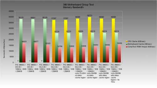
| Processor Cache Thruput (KBytes/sec) | 0 | 0 | 0 | 37287 | 37287 | 38490 | 39773 | 38490 | 38490 |
| Motherboard Cache | 256KB | 256KB | 256KB | 256KB | 256KB | 256KB | 256KB | 256KB | 256KB |
| Motherboard Cache Thruput (KBytes/sec) | 38125 | 38001 | 38129 | 25735 | 25770 | 26009 | 26018 | 26016 | 26018 |
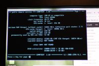
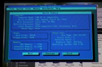
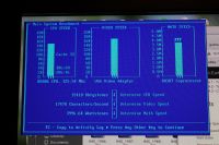
| Norton Sysinfo CPU | 43.0 | 43.0 | 48.5 | 65.3 | 65.4 | 65.5 | 65.5 | 65.5 | 65.5 |
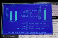
| Norton Sysinfo HDD (KBytes/sec) | 934 | 1060 | 826 | N/A | 990 | N/A | N/A | N/A | N/A |
| Norton Sysinfo Overall | 31.3 | 31.6 | 34.8 | N/A | 46.4 | N/A | N/A | N/A | N/A |
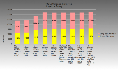
| CheckIt Dhrystones | 11430 | 11631 | 13812 | 15418 | 15418 | 15418 | 15418 | 15418 | 15785 |
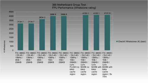
| CheckIt Whetstones | 3134.7 | 3134.7 | 3634.3 | 3996.6 | 3996.6 | 4125.1 | 4125.1 | 4131.9 | |
| CheckIt Video chars/sec VGA 1 | 19067 | 19420 | 20167 | 22313 | 22798 | ||||
| CheckIt Video chars/sec VGA 2 | 20563 | 20974 | 21402 | 23834 | 23834 | ||||
| CheckIt Video chars/sec VGA 3 | 16646 | FAILED | 15652 | 17478 | FAILED | FAILED | 19067 | 19067 | 19067 |
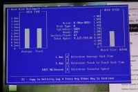
| CheckIt HDD Transfer | 921.1 | 1037.9 | 801 | 877.2 | 1151.4 | ||||
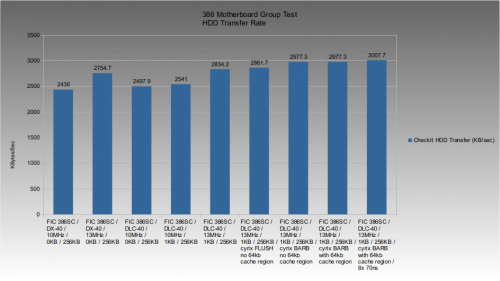
| CheckIt HDD Transfer, with shadowed XT-IDE BIOS | 2436.0 | 2754.7 | 2497.9 | 2541.0 | 2834.2 | 2861.7 | 2977.3 | 2977.3 | 3007.7 |
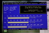
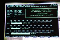
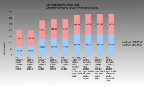
| Landmark CPU (effective MHz vs IBM AT) | 69.39 | 69.39 | 128.47 | 134.05 | 134.06 | 167.49 | 167.50 | 167.49 | 167.49 |
| Landmark FPU (effective MHz vs IBM AT) | 130.12 | 129.93 | 150.77 | 155.02 | 154.94 | 156.65 | 161.69 | 161.68 | 162.16 |
| Landmark Video VGA 1 | 2908.4 | 2969.91 | 2899.82 | 2899.82 | 2969.91 | ||||
| Landmark Video VGA 2 | 4292.75 | 5782.59 | 4818.82 | 4818.82 | 5782.59 | ||||
| Landmark Video VGA 3 | 4818.82 | 5782.59 | 4818.82 | 4818.82 | 5782.59 | 5921.93 | 5921.93 | 5921.93 | 5921.93 |
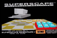
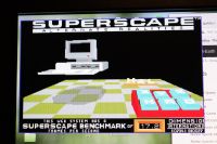
| 3DBench VGA 1 (fps) | 15.1 | 15.3 | 17.8 | 19.6 | 20.0 | ||||
| 3DBench VGA 2 (fps) | 16.3 | 17.2 | 20.4 | 22.7 | 23.2 | ||||
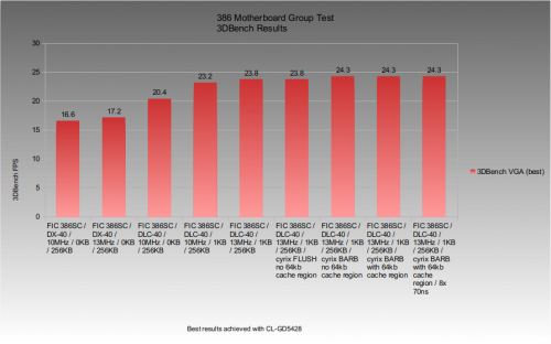
| 3DBench VGA 3 (fps) | 16.6 | 17.2 | 20.4 | 23.2 | 23.8 | 23.8 | 24.3 | 24.3 | 24.3 |
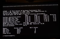
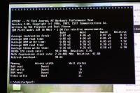
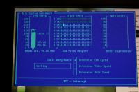
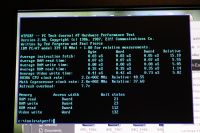
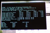
| ATPerf RAM Read wait states | 0 | 0 | 6 | 21 | 21 | 6 | 22 | 22 | 30 |
| ATPerf RAM Write wait states | 0 | 0 | 23 | 23 | 23 | 22 | 22 | 22 | 15 |
| ATPerf ROM Read wait states | 10 | 10 | 96 | 112 | 112 | 95 | 88 | 88 | 59 |
| ATPerf Video Write VGA 1 | 25 | 24 | 221 | 221 | 217 | ||||
| ATPerf Video Write VGA 2 | 16 | 11 | 132 | 133 | 110 | ||||
| ATPerf Video Write VGA 3 | 14 | 132 | 132 | 110 | 107 | 108 | 108 | 108 | |
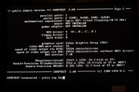
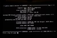
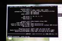
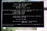
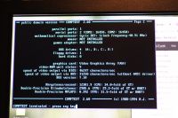
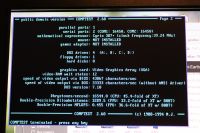
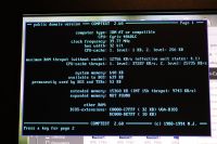
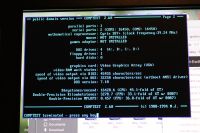
| CompTest RAM thruput | 16933 | 16877 | 15320 | 12756 | 12800 | 13006 | 14053 | 14052 | 15438 |
| CompTest Effective WS | 2.6 | 2.7 | 3.1 | 4.1 | 4.1 | 4.0 | 3.6 | 3.6 | 3.1 |
| CompTest MFLOPS | 0.395 | 0.392 | 0.422 | 0.455 | 0.457 | 0.449 | 0.478 | 0.478 | 0.478 |
| CompTest Video BIOS VGA 1 | 66473 | 66845 | 71023 | 78241 | 78241 | ||||
| CompTest Video BIOS VGA 2 | 64496 | 64847 | 62145 | 67222 | 67794 | ||||
| CompTest Video BIOS VGA 3 | 44272 | 46247 | 40242 | 43867 | 45455 | 45804 | 48307 | 49102 | 52563 |
| CompTest Video Direct VGA 1 | 25000 | 25000 | 27027 | 27778 | 27778 | ||||
| CompTest Video Direct VGA 2 | 32258 | 33333 | 29412 | 30303 | 30303 | ||||
| CompTest Video Direct VGA 3 | 31250 | 31250 | 33333 | 33333 | 32258 | 29412 | 31250 | 35714 | 35714 |
| CompTest Dhrystones | 12417.1 | 12444.4 | 14534.3 | 16544.0 | 16428.6 | 16448 | 16448 | 16464 | 16595.2 |
Games Results
In addition, the following game benchmark results were recorded:
| Test | Config 0 | Config 1 | Config 2 | Config 3 | Config 4 | Config 5 | Config 6 | Config 7 | Config 8 |
|---|---|---|---|---|---|---|---|---|---|
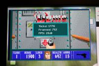
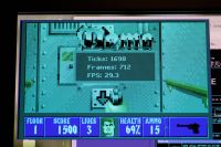
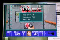
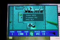
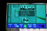
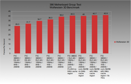
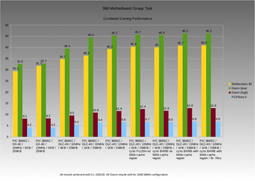
| Wolfenstein 3D (FPS) | 29.3 | 31.7 | 34.7 | 36.3 | 39.2 | 40.3 | 40.0 | 40.7 | 40.9 |
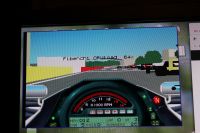
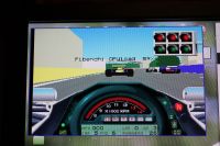
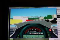
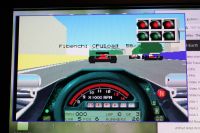
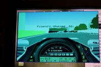
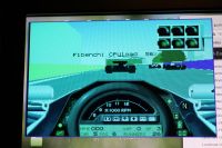
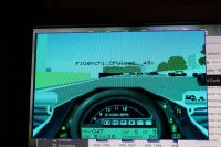
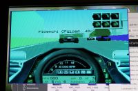
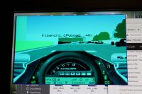
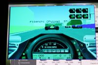
| F1GP Bench 1 (CPU %) | 59-64 | 56-62 | 48-51 | 40-43 | 37-40 | 37-40 | 37-40 | 37-40 | |
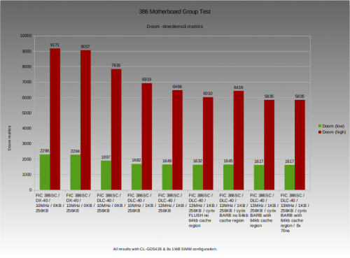
| Doom timedemo 3 (low detail) | 2298 / 32.5fps | 2284 / 32.7fps | 1897 / 39.4fps | 1682 / 44.4fps | 1649 / 45.2fps | 1632 / 45.7fps | 1645 / 45.4fps | 1617 / 46.2fps | 1617 / 46.2fps |
| Doom timedemo 3 (high detail) | 9171 / 8.1fps | 9057 / 8.2fps | 7835 / 9.5fps | 6919 / 10.8fps | 6468 / 11.5fps | 6010 / 12.4fps | 6419 / 11.6fps | 5835 / 12.8fps | 5835 / 12.8fps |
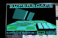
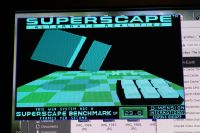
| PC Player benchmark | 4.2fps | 4.2fps | 5.4fps | 6.4fps | 6.6fps | 6.7fps | 6.6fps | 6.8fps | 6.8fps |
Software Versions
- Norton Sysinfo 8.0
- CheckIt 2.1
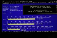
- Landmark 6.00
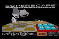
- 3DBench 1.0
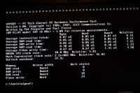
- ATPerf 2.00
- Comptest 260
- Doom 1.9
Notes
- Doom FPS figures are calculated as: (35 * 2134)/realtics = fps , where 2134 is the fixed number of 'tics' in the 'timedemo3' playthrough.
- Doom benchmarks were all gained using the 8x 1MB memory configuration at 1ws, as it turned out that the 4x 4MB 60ns configuration was unstable with Doom. This config does have a memory throughput benefit compared to the other configuration, so the Doom scores are mainly to compare the difference in cyrix.exe cpu cache tweaking and the DX vs DLC differences.
- Fastest gaming scores were achieved using VGA 3 - the Cirrus Logic card; at all real-world tests it is consistently faster (although by a negligible amount in some cases) than the ET4000 card. Synthetic tests are really not clear at all (even the Trident card is faster in some of those, and we know that the Trident 9000 is nowhere near in reality).
- During testing I found that the Cirrus Logic card had a damaged trace near the VGA connector; I'm certain this is responsible for the blue-tinged output. It will get repaired and appears to have no impact on the performance of the card.
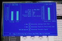
- After the first few rounds of testing I was able to work out how to shadow the XTIDE BIOS from slow ROM to the 640-1024K reserved region, as used by VGA and System shadow functionality. By doing this the IDE transfer speeds increased by well over 100%. I've added these results in a second row against the CheckIT HDD transfer data.
Conclusion
CPU
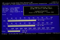
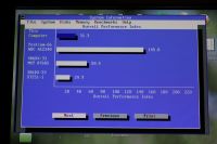
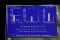
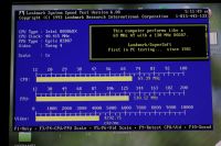
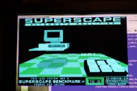
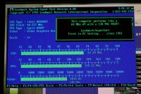
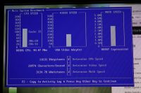
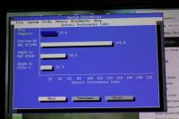
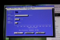
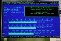
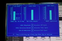
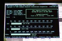
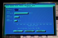
Synthetic CPU/FPU scores from Landmark:
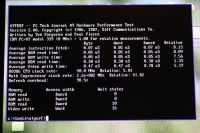
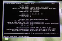
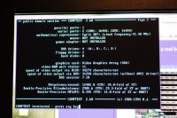
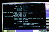
Dhrystone and Whetstone integer and floating point metrics from CheckIt:
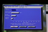
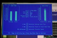
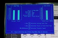
Disk IO
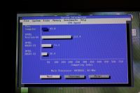
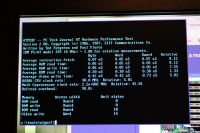
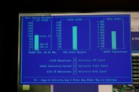
Memory & Cache
Gaming
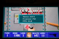
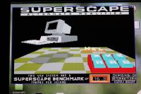
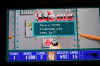
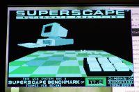
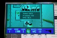
Results from Wolfenstein 3D special benchmark version, as well as 3DBench:
Results from the Doom -timedemo 3 game benchmark:
Combined results of all gaming benchmarks:
Final Thoughts
- Testing proves that the Cirrus Logic card is as-fast-as or faster-than the Tseng Labs ET4000AX in every real-world benchmark. That's no surprise as it's a much later design.
- The Am386DX-40 really doesn't benefit much from the ISA overclock to 13MHz; in Doom it is clearly the processor that is by far the most restrictive element.
- The Tx486DLC-40 going from cpu cache-disabled to the default cpu cache-enabled setting results in a 12% improvement in Doom low-detail frame rates and 13% in high-detail.
- The Tx486DLC-40 going from cpu cache-disabled to the most optimised cache-enabled setting results in a 17% improvement in Doom low-detail frame rates and a staggering 35% improvement at high-detail.
- Boosting the ISA clock from 10MHz to 13MHz with the DLC brings just a 1% improvement to Doom low-detail frame rates (to be expected, since we're not pushing many pixels!) but more than 6% in high-detail. In certain benchmarks this is noticeable, but in the real world many ISA cards would be way out-of-spec at such a setting; in that case the 10MHz ISA clock is a good, stable increase over the ISA 'default' standard of ~8MHz.
- From non-optimised cache-enabled settings to most-optimised shows gains over just under 5% in low-detail modes and 19% in high-detail Doom timedemo results. Who wouldn't want a free 19% of extra performance!
This is a really nice 386DX board - it has plenty of expansion slots, supports up to 256KB of cache, and natively detects and supports the DLC-series of 386-486 processors from Cyrix and Texas Instruments. To get the best performance from the DLC processors you really must use the cyrix.exe cache control utility as the basic support from the motherboard BIOS really does not let it shine.
With the MR BIOS ROM fitted there are a good range of optimisation settings available and it performs well (very well, in fact) at virtually every setting. At the most-optimised settings with the 486DLC-40 and a Cirrus Logic GD5428 it equals the best recorded scores for other DLC-supporting 386 motherboards and is within a hairs breadth of full 486DX-33 systems.
For folks who had a 386 originally, the upgrade path of this board to the DLC processors would have been very, very tempting.
At some point I would like to try to find a Tx486SXL-40 or Tx486SXL2-50, since they contain 8KB of cache compared to the 1KB of the DLC. But other than that, this is about as far as you can really go with a true 386 design.
(Go back to the 386 PC main page)
