Biostar MB-1220VE (VLSI VL82C311L)
A 286 motherboard that I bought from an auction site. With overview of specifications, the repairs it needed and benchmarks & testing.
Initial Thoughts
This was a board that I had come across whilst searching for the “latest and greatest” 286 designs - these were usually those boards that came out whilst the 386 was firmly established, often crossing the line of features normally found on low to mid range 386SX systems.
The key features about 286 boards in this era were:
- Very low chipset count; other than a few discrete logic chips (the odd 74-series), most boards have a CPU socket, FPU, BIOS ROM and just one or two larger IC's making up the motherboard chipset - these integrated the interrupt controller, DMA and memory controller, timers and often keyboard controllers. Parts which were usually served by one or more individual chips on early designs.
- Usually SIMM (though sometimes SIPP) sockets with almost all models supporting at least 4MB, sometimes more.
- Minimum of 16MHz 80286 processor support.
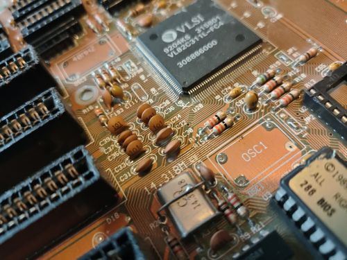
The Headland HT12 falls into this category, as well as some Suntac and Chips & Technologies designs. The chipset that VLSI used to cross the 286/386 barrier was the VL82C311, or more specifically the VL82C311L for the 286-specific implementation.
The Biostar MB-1220VE caught my eye when I found an old forum post where an owner of such a board posted a screenshot of the all the various BIOS settings which looked far more like a like model 386; especially all of the optimisation settings. When I did a bit more research I found that the board supported 16MB of SIMM memory and at least 20MHz processors as standard (although the Eurosoft HT12 ran reliably at 20MHz, it was outside of its specifications in doing so). This gives us hope that a 'good' one may be able to go a bit higher.
Sadly, unlike the ever present HT12 boards, or the older VLSI multi-chip designs, this one being a very late board that most people would have passed on in favour of a 386 or better, is not very common at all.
To my surprise, whilst searching through various pages of hits on Google, I found a Russian auction site with a seller who appeared to have one for sale….
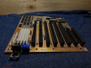
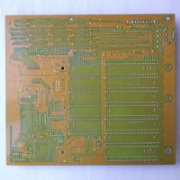
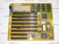
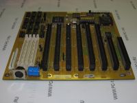
Original Auction Images
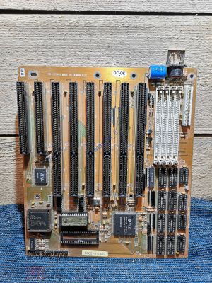
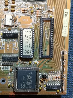
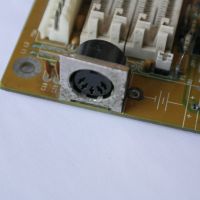
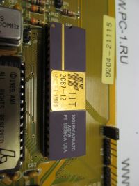
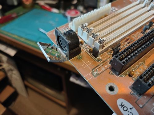
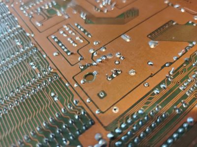
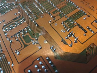
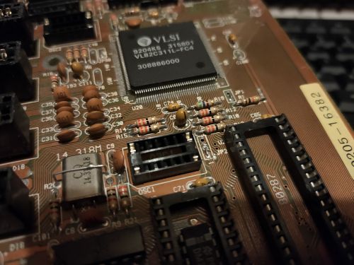
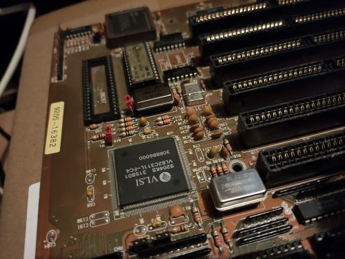
The board has clearly seen better days - there are at least a few traces that have been scratched through, the ISA sockets look a bit chewed up, the shield around the AT keyboard port is hanging off and it looks like it is missing the two oscillators (16MHz for the FPU and 40MHz for the 20MHz Harris CPU).
None of those are major issues as they are all repairable. The big bonus is that looking around the battery there didn't appear to be any evidence of leaks - that's the main killer of these old boards.
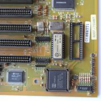
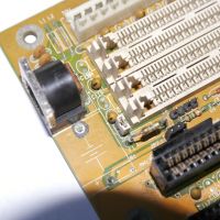
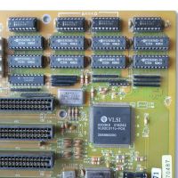
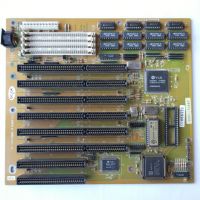
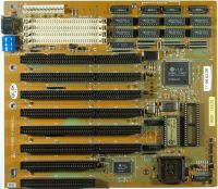
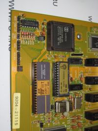
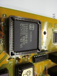
Additional Images
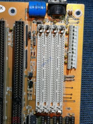
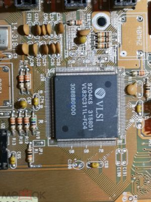
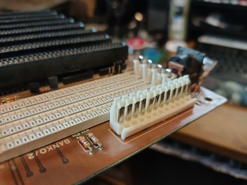
These are not my images, but others I've found of the MB-1220VE out on the web, there are various close-ups which may or may not be useful given that this is quite a rare motherboard:
Arrival Pictures
[Update 10/03/2021] Motherboard arrived from Russia
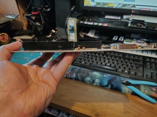
First of all… it's warped. Bent like a banana!
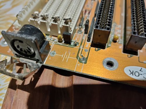
Secondly, it's actually not in too bad a shape. I think we've caught the battery just in time - there are signs of corrosion just at the base of the battery tabs, but nowhere else:
The oscillators have been robbed from the board - it's very obvious that they've been desoldered:
There's some very minor damage to the P8/P9 power header, but nothing that should affect its operation:
Motherboard Data & Variants
A summary of the motherboard capabilities follows:
| Item | MB-1220VE | MB-1220VE v0.1 |
|---|---|---|
| Form Factor | Baby AT | Baby AT |
| Chipset | VLSI VL82C311L (SCAMP-DT 286) | VLSI VL82C311L (SCAMP-DT 286) |
| Dimensions | 220mm x 220mm | 249mm x 221mm |
| Maximum RAM | 16MB | 16MB |
| FPU | Yes | Yes |
| CPU Speeds | 16/20MHz | 16/20/25MHz* |
| Expansion | 6x16bit, 2x8bit | 6x16bit, 2x8bit |
*Not entirely sure this is accurate, based on the VLSI datasheet.
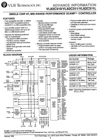
Data on the VLSI VL82C311 (and -L variant) chipset can be found below:
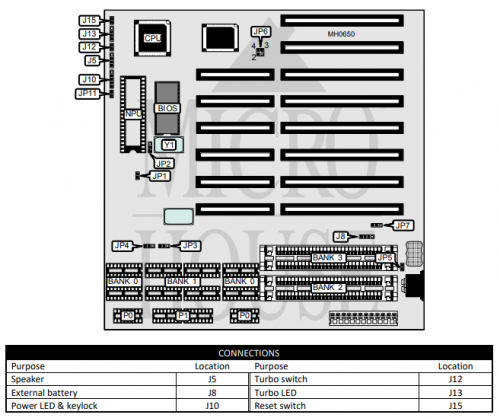
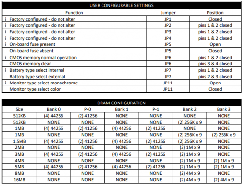
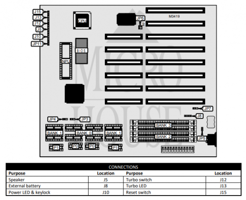
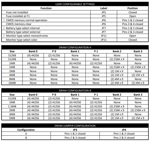
Motherboard jumper settings can be found in the following locations:
Note that there are two minor variations of this motherboard, identified simply as MB-1220VE and MV-1220VE v.01. There appears to be little in the way of visual differences between the two, with the only major change being the positioning of Bank 0 of the DIP RAM sockets;
- According to the configuration details from the above sites (and reproduced below), on the original board Bank 0 are the two outer pairs of DIP sockets.
- On the v.01 board Bank 0 appears to be the middle pairs of DIP sockets.
Some later revision boards have the rev.01 silk screened on the board, but from the images I've seen, not all of them do.
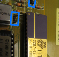
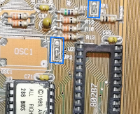
The only other tell-tale signs between the variants are that the v.01 board is missing jumpers JP1 and JP2, next to the BIOS/FPU sockets:
The left board appears to be the original version, with the headers, whereas the v.01 board on the right these are hard-wired links.
Other than the layout of Bank 0 of the DIP sockets, I'm not entirely convinced that there is any technical differences between the two systems. One set of data implies that the v.01 board supports up to 25MHz processors, but the chip data for the VLSI 82C311L says that the -FC suffixed parts are only 20MHz rated. And the -FC part is present on both v.0 and v.01 boards and the VLSI datasheet only lists the -25 parts for the 386SX variant…. so, it's anyone's guess, really.
BIOS
BIOS from my motherboard:
Repairs
First job was to remove the barrel battery and do an initial cleanup of the small amount of corrosion present at the base of the battery tabs:
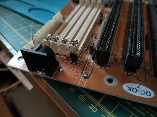
Next I'll need to remove the keyboard socket and repair those battery terminal tabs and any other corrosion around the area (which isn't a lot).
Below: Keyboard socket replaced and battery tab solder points re-filled:
Below: DIL-14 sockets fitted in place of the original oscillator solder pads and 40MHz and 32MHz cans pushed in:
So, did it work?
Well…..
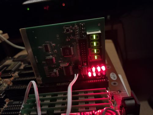
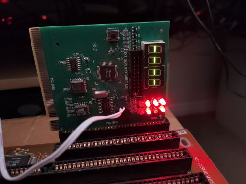
The POST diagnostic card indicates reset held high and no CLK signal 
[Update 14/03/2021] - I swapped the processor on a chance it was faulty…
The held reset light now goes out, and the CLK light stays lit. So that's an improvement. Still no error codes though.
Further Testing
Clock Signals
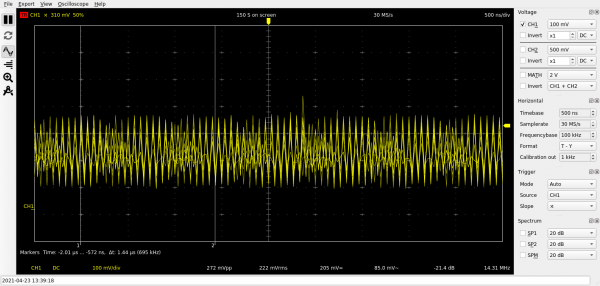
The 14MHz oscillator which was still fitted to the board on receiving it is working; the clock is present on the output pin from the can as well as on ISA socket pin B30 (OSC):
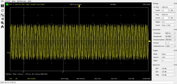
There is an 8MHz clock present on ISA socket pin B20 (CLK):
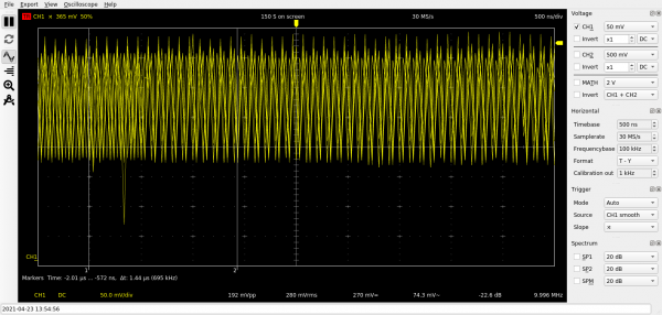
Processor pin 31 (CLK) has a 9.996MHz clock:
This doesn't seem correct. The processor is a 20MHz unit, and is being driven, as is normal on a 286, by a standard DIL can oscillator of 2x the processor frequency (i.e. 40MHz). The definition for pin 31 is that it “is divided by 2 internally within the processor to generate the processor clock” (from the AMD 80286 datasheet)… that would mean the processor is only at 5MHz. Unless I misunderstand the datasheet, something is drastically wrong here.
Configuration
V.0 Motherboard
V.01 Motherboard
0 Wait State & Further BIOS Optimisation
Math Co-Processor
Speed Testing & Tuning
Configuration 0
- Harris CS80C286-25
- 32MHz oscillator (16MHz CPU speed)
- BIOS and wait states unoptimised
- Standard ISA bus clock
- 4x 1MB 60ns SIMM
- VGA 1 Trident TVGA9000 512KB VGA
- VGA 2 Tseng Labs ET4000AX 1MB VGA
This a baseline configuration with zero-wait, standard ISA bus timings and BIOS shadowing disabled. It is intended as a 'worst-case', 'maximum stability' comparison.
Configuration 1
- Harris CS80C286-25
- 32MHz oscillator (16MHz CPU speed)
- 0-wait states + BIOS optimisation
- System + Video BIOS shadowed
- 4x 1MB 60ns SIMM
- VGA 1 Trident TVGA9000 512KB VGA
- VGA 2 Tseng Labs ET4000AX 1MB VGA
Configuration 2
- Harris CS80C286-25
- 40MHz oscillator (20MHz CPU speed)
- 0-wait states + BIOS optimisation
- System + Video BIOS shadowed
- 4x 1MB 60ns SIMM
- VGA 1 Trident TVGA9000 512KB VGA
- VGA 2 Tseng Labs ET4000AX 1MB VGA
Configuration 3
- Harris CS80C286-25
- 48MHz oscillator (24MHz CPU speed)
- 0-wait states + BIOS optimisation
- System + Video BIOS shadowed
- 4x 1MB 60ns SIMM
- VGA 1 Trident TVGA9000 512KB VGA
- VGA 2 Tseng Labs ET4000AX 1MB VGA
Configuration 4
- Harris CS80C286-25
- 50MHz oscillator (25MHz CPU speed)
- 0-wait states + BIOS optimisation
- System + Video BIOS shadowed
- 4x 1MB 60ns SIMM
- VGA 1 Trident TVGA9000 512KB VGA
- VGA 2 Tseng Labs ET4000AX 1MB VGA
Configuration 5
- Harris CS80C286-25
- 54MHz oscillator (27MHz CPU speed)
- 0-wait states + BIOS optimisation
- System + Video BIOS shadowed
- 4x 1MB 60ns SIMM
- VGA 1 Trident TVGA9000 512KB VGA
- VGA 2 Tseng Labs ET4000AX 1MB VGA
Configuration 6
- Harris CS80C286-25
- 56MHz oscillator (28MHz CPU speed)
- 0-wait states + BIOS optimisation
- System + Video BIOS shadowed
- 4x 1MB 60ns SIMM
- VGA 1 Trident TVGA9000 512KB VGA
- VGA 2 Tseng Labs ET4000AX 1MB VGA
Results
| Test | Config 0 | Config 1 | Config 2 | Config 3 | Config 4 | Config 5 | Config 6 |
|---|---|---|---|---|---|---|---|
| Processor Speed | 16MHz | 16MHz | 20MHz | 24MHz | 25MHz | 27MHz | 28MHz |
| Wait states | 1 | 0 | 0 | 0 | 0 | 0 | 0 |
| Norton Sysinfo CPU | |||||||
| Norton Sysinfo HDD | |||||||
| Norton Sysinfo Overall | |||||||
| CheckIt Dhrystones | |||||||
| CheckIt Whetstones | |||||||
| CheckIt Video chars/sec VGA 1 | |||||||
| CheckIt Video chars/sec VGA 2 | |||||||
| CheckIt HDD Transfer | |||||||
| Landmark CPU | |||||||
| Landmark FPU | |||||||
| Landmark Video VGA 1 | |||||||
| Landmark Video VGA 2 | |||||||
| 3DBench VGA 1 | |||||||
| 3DBench VGA 2 | |||||||
| ATPerf RAM Read | |||||||
| ATPerf RAM Write | |||||||
| ATPerf ROM Read | |||||||
| ATPerf Video Write VGA 1 | |||||||
| ATPerf Video Write VGA 2 | |||||||
| CompTest RAM thruput | |||||||
| CompTest Effective WS | |||||||
| CompTest MFLOPS | |||||||
| CompTest Video BIOS VGA 1 | |||||||
| CompTest Video BIOS VGA 2 | |||||||
| CompTest Video Direct VGA 1 | |||||||
| CompTest Video Direct VGA 2 | |||||||
| CompTest Dhrystones |
Games Results
In addition, the following game benchmark results were recorded:
| Test | Config 0 | Config 1 | Config 2 | Config 3 | Config 4 | Config 5 | Config 6 |
|---|---|---|---|---|---|---|---|
| Wolfenstein 3D (FPS) | |||||||
| F1GP Bench 1 (CPU %) |
Software Versions
- Norton Sysinfo 8.0
- CheckIt 2.1
- Landmark 6.00
- 3DBench 1.0
- ATPerf 2.00
- Comptest 260
Notes
Conclusion
(Go back to the 286 PC main page)

